In the quotation of Mass PCBA Production, the cost of the PCBA Test Jig usually appears. However, many customers do not really understand what PCBA Test Jig is; Now, let’s find the answer!
What Is PCBA Test Jig?
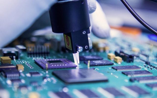
The principle of the PCBA test jig is quite simple. It connects the pads or test points on the Printed Circuit Board (PCB ) through metal probes. When the PCB board is powered on, the voltage value and current value of the test circuit are able to be obtained, then to observe whether the circuit is normal or not.
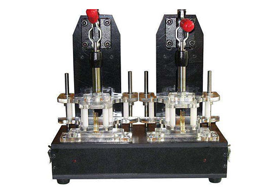
The production of PCBA test jig is all custom-made, which is determined according to the size of the PCB to be tested, the location of the test point, and the value to be tested. Mainly use acrylic, plastic, metal probe, display screen, wire and simple PCB circuit board to complete the whole PCBA Test Jig manufacturing.
The Purpose of PCBA Test JIg
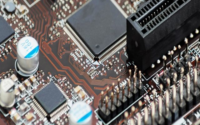
The PCBA test jig is widely used in the entire PCBA manufacturing process. It is mainly used to test the PCBA board after assembled PCB (SMT and DIP Soldering). Among them, ICT test is the main method, that is, the electrical conductivity of the circuit board is tested through test points. Through the performance, so as to determine whether the entire PCB board is successfully welded. The PCBA test jig is the main tool used to assist in completing this test.
The quality of the PCBA test jig is related to the efficiency and first pass rate of ICT test. Due to its long-term frequent operation, it has high requirements for its production quality, and PCBA manufacturers need to pay sufficient attention to it.