In integrated circuit application design, after the project schematic design is completed, PCB design is required. Because it is a crucial link. The quality of the design result directly affects the entire design function. Therefore, a reasonable and efficient PCB Layout is a key step for successful chip circuit design and debugging.
1) Component package selection
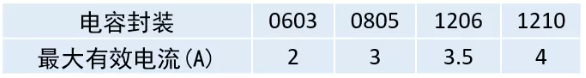
Resistance selection: The voltage resistance, maximum power consumption and temperature of the selected resistance cannot exceed the use range.
Capacitor selection: When selecting, you also need to consider the withstand voltage and maximum effective current of the selected capacitor.
Inductor selection: The effective value current and peak current of the selected inductor must be greater than the current in the actual circuit.
2)Common interference in circuit design
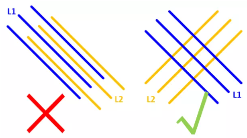
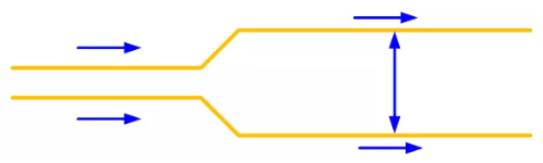
Crosstalk: When the parallel wiring distance of the design line is too long, the capacitance and mutual inductance between the wires will couple energy to the adjacent transmission line. The effects of crosstalk can be reduced by the following methods:
1. Join the safe routing

2. In practice, try to make adjacent traces perpendicular to each other
3. Every time you walk a distance of parallel lines, increase the distance between the two lines
Reflection: The impedance mismatch of the transmission line due to too many bends and branches in the wiring can be improved by reducing the bends and branch lines on the line or avoiding right-angle wiring and branch line reinforcement.
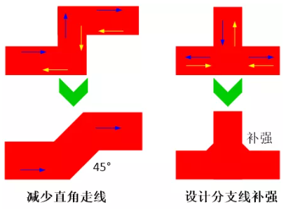
The impedance mismatch of the transmission line due to the wiring corners and too many branches can be improved by reducing the corners and branch lines on the line or avoiding right-angle wiring and branch line reinforcement.
3)Determine the grounding method
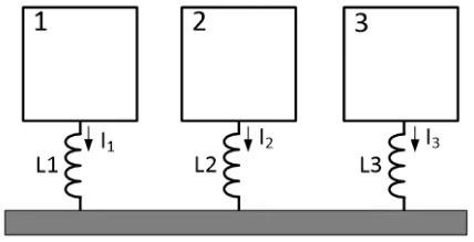
Single-point grounding (applicable to low-frequency circuits): All circuit grounding wires are connected to the same point of the common grounding wire, the wiring is simple, and the mutual interference of ground loops is reduced.
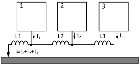
Multi-point grounding (applicable to multilayer circuit/high-frequency circuit): each part of the system is grounded nearby to provide low ground impedance.
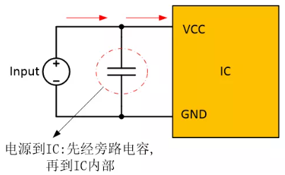
Add filtering and bypass capacitors
To ensure a stable input/output voltage, add input/output capacitors.
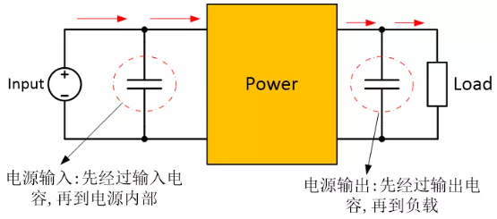
Add a bypass capacitor between the power supply and the IC to ensure a stable input voltage and filter out high-frequency noise.
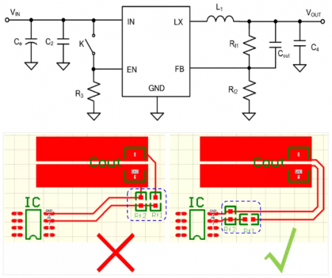
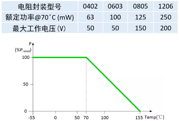
4)Impedance position design
In contrast, the higher the impedance, the more susceptible to interference. The following is the PCB impedance position design of the synchronous buck chip.